
《德源科技》r)Pololu 12V 600mA Step-Down Voltage D24V6F12
Regulator
$260
運費抵用券7-ELEVEN 滿99元運費折抵31元
- 現金付款
- 全家取貨付款
- 7-ELEVEN取貨付款
現金付款
- Yahoo奇摩輕鬆付現金接受付款方式:ATM轉帳 / Famiport / 輕鬆付帳戶餘額
ATM 提供5家銀行:合作金庫、華南銀行、台灣銀行、國泰世華、中國信託,以上5家同行轉帳,免轉帳手續費。
全家取貨付款
— Yahoo奇摩輕鬆付7-ELEVEN取貨付款
— Yahoo奇摩輕鬆付7-ELEVEN取貨付款 — 單件運費$60、滿10件或消費滿$20000免運費
- 單件運費$60
- 滿2件,運費$60
- 滿3件,運費$60
- 滿10件或消費滿$20000免運費
全家取貨付款 — 單件運費$60、滿10件或消費滿$20000免運費
- 單件運費$60
- 滿2件,運費$60
- 滿3件,運費$60
- 滿10件或消費滿$20000免運費
郵寄掛號 — 單件運費$60、滿10件或消費滿$20000免運費
- 單件運費$60
- 滿2件,運費$60
- 滿3件,運費$60
- 滿10件或消費滿$20000免運費

輕鬆付提供價金保管,交易更安心!
商品資訊
下標前請注意: (請先打電話連絡或提問,請見賣方關於我中有聯絡方式)
1.可以開發票
(PS:如合併結帳多項產品或是加購附件及開發票者,使用全家取貨付款的,結標後請自行修改金額)
2.可面交,現貨供應
3.下標後請填寫下列資料
1.帳號:
2.購買物品名稱:(如有很多型號時請註明清楚,謝謝)
3.地址:
4.郵遞區號:
5.郵款金額:
6.姓名:
7.帳號後5碼:
8.連絡電話:
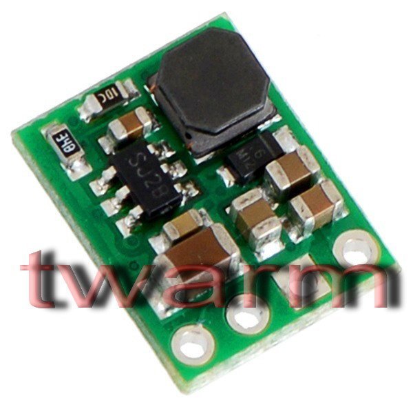
=================================================================== id=6452 ※本產品原廠代理從國外進口,有些交期較長,下訂前請詢問! The compact (0.32"×0.515") U3V12F12 switching step-up (or boost) voltage regulator takes an input voltage as low as 2.5 V and efficiently boosts it to 12 V. The pins have a 0.1" spacing, making this board compatible with standard solderless breadboards and perfboards. These boost (step-up) voltage regulators generate higher output voltages from input voltages as low as 2.5 V. They are switching regulators (also called switched-mode power supplies (SMPS) or DC-to-DC converters) and have a typical efficiency between 80% to 90%. The available output current is a function of the input voltage, output voltage, and efficiency (see Typical Efficiency and Output Current section below), but the input current can typically be as high as 1.4 A. This regulator is available with a fixed 5 V, 9 V, or 12 V output: The regulator’s thermal shutdown prevents damage from overheating, but it does not have short-circuit or reverse-voltage protection. We have several other boost regulators that you might consider as alternatives to these: The boost regulator has three connections: input voltage (VIN), ground (GND), and output voltage (VOUT). The input voltage, VIN, must be at least 2.5 V and should not exceed the output voltage, VOUT. Please be wary of destructive LC spikes that might cause the input voltage to exceed VOUT (see below for more information). The three connections are labeled on the back side of the PCB, and they are arranged with a 0.1" spacing along the edge of the board for compatibility with solderless breadboards, connectors, and other prototyping arrangements that use a 0.1" grid. You can solder wires directly to the board or solder in either the 3×1 straight male header strip or the 3×1 right-angle male header strip that is included. The efficiency of a voltage regulator, defined as (Power out)/(Power in), is an important measure of its performance, especially when battery life or heat are concerns. As shown in the graphs below, this switching regulator typically has an efficiency of 80 to 90%. The maximum achievable output current is approximately proportional to the ratio of the input voltage to the output voltage. If the input current exceeds the switch current limit (typically somewhere between 1.4 and 2 A), the output voltage will begin to drop. Additionally, the maximum output current can depend on other factors, including the ambient temperature, air flow, and heat sinking. When connecting voltage to electronic circuits, the initial rush of current can cause damaging voltage spikes that are much higher than the input voltage. In our tests with typical power leads (~30" test clips), input voltages above 10 V caused voltage spikes in excess of 20 V. You can suppress such spikes by soldering a 33μF or larger electrolytic capacitor close to the regulator between VIN and GND. More information about LC spikes can be found in our application note, Understanding Destructive LC Voltage Spikes.

Overview


Features
Using the Regulator
Connections

Typical Efficiency and Output Current

LC Voltage Spikes
